- 您现在的位置:买卖IC网 > Sheet目录3855 > PIC16LC711-04/SS (Microchip Technology)IC MCU OTP 1KX14 A/D 20SSOP
PIC16C71X
DS30272A-page 16
1997 Microchip Technology Inc.
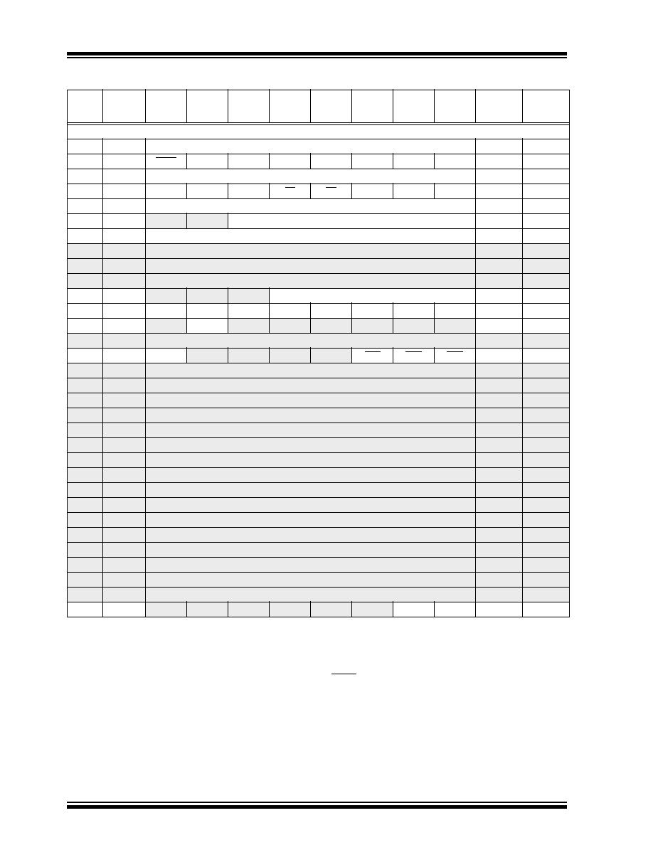
Bank 1
80h(1)
INDF
Addressing this location uses contents of FSR to address data memory (not a physical register)
0000 0000
81h
OPTION
RBPU
INTEDG
T0CS
T0SE
PSA
PS2
PS1
PS0
1111 1111
82h(1)
PCL
Program Counter's (PC) Least Signicant Byte
0000 0000
83h(1)
STATUS
IRP(4)
RP1(4)
RP0
TO
PD
Z
DC
C
0001 1xxx
000q quuu
84h(1)
FSR
Indirect data memory address pointer
xxxx xxxx
uuuu uuuu
85h
TRISA
—
PORTA Data Direction Register
--11 1111
86h
TRISB
PORTB Data Direction Register
1111 1111
87h
—
Unimplemented
—
88h
—
Unimplemented
—
89h
—
Unimplemented
—
8Ah(1,2)
PCLATH
—
Write Buffer for the upper 5 bits of the PC
---0 0000
8Bh(1)
INTCON
GIE
PEIE
T0IE
INTE
RBIE
T0IF
INTF
RBIF
0000 000x
0000 000u
8Ch
PIE1
—
ADIE
—
-0-- ----
8Dh
—
Unimplemented
—
8Eh
PCON
MPEEN
—
PER
POR
BOR
u--- -1qq
u--- -1uu
8Fh
—
Unimplemented
—
90h
—
Unimplemented
—
91h
—
Unimplemented
—
92h
—
Unimplemented
—
93h
—
Unimplemented
—
94h
—
Unimplemented
—
95h
—
Unimplemented
—
96h
—
Unimplemented
—
97h
—
Unimplemented
—
98h
—
Unimplemented
—
99h
—
Unimplemented
—
9Ah
—
Unimplemented
—
9Bh
—
Unimplemented
—
9Ch
—
Unimplemented
—
9Dh
—
Unimplemented
—
9Eh
—
Unimplemented
—
9Fh
ADCON1
—
PCFG1
PCFG0
---- --00
TABLE 4-2:
PIC16C715 SPECIAL FUNCTION REGISTER SUMMARY (Cont.’d)
Address Name
Bit 7
Bit 6
Bit 5
Bit 4
Bit 3
Bit 2
Bit 1
Bit 0
Value on:
POR,
BOR, PER
Value on all
other resets
(3)
Legend: x = unknown, u = unchanged, q = value depends on condition, - = unimplemented read as '0'.
Shaded locations are unimplemented, read as ‘0’.
Note 1:
These registers can be addressed from either bank.
2:
The upper byte of the program counter is not directly accessible. PCLATH is a holding register for the PC<12:8> whose
contents are transferred to the upper byte of the program counter.
3:
Other (non power-up) resets include external reset through MCLR and Watchdog Timer Reset.
4:
The IRP and RP1 bits are reserved on the PIC16C715, always maintain these bits clear.
发布紧急采购,3分钟左右您将得到回复。
相关PDF资料
PIC18F65K22-I/MRRSL
MCU PIC 32K FLASH MEM XLP 64QFN
PIC16LF87-I/SS
IC MCU FLASH 4KX14 EEPROM 20SSOP
PIC16C62B-20/SS
IC MCU OTP 2KX14 PWM 28SSOP
PIC16LC711-04I/SO
IC MCU OTP 1KX14 A/D 18SOIC
PIC18F66J90-I/PT
IC PIC MCU FLASH 64KB 64-TQFP
ATMEGA32L-8AC
IC AVR MCU 32K LV 8MHZ COM44TQFP
DSPIC30F2012-30I/SP
IC DSPIC MCU/DSP 12K 28DIP
PIC18LF2321-I/ML
IC PIC MCU FLASH 4KX16 28QFN
相关代理商/技术参数
PIC16LC711-04E/P
功能描述:8位微控制器 -MCU 1.75KB 68 RAM 13 I/O RoHS:否 制造商:Silicon Labs 核心:8051 处理器系列:C8051F39x 数据总线宽度:8 bit 最大时钟频率:50 MHz 程序存储器大小:16 KB 数据 RAM 大小:1 KB 片上 ADC:Yes 工作电源电压:1.8 V to 3.6 V 工作温度范围:- 40 C to + 105 C 封装 / 箱体:QFN-20 安装风格:SMD/SMT
PIC16LC711-04E/SO
功能描述:8位微控制器 -MCU 1.75KB 68 RAM 13 I/O RoHS:否 制造商:Silicon Labs 核心:8051 处理器系列:C8051F39x 数据总线宽度:8 bit 最大时钟频率:50 MHz 程序存储器大小:16 KB 数据 RAM 大小:1 KB 片上 ADC:Yes 工作电源电压:1.8 V to 3.6 V 工作温度范围:- 40 C to + 105 C 封装 / 箱体:QFN-20 安装风格:SMD/SMT
PIC16LC711-04E/SS
功能描述:8位微控制器 -MCU 1.75KB 68 RAM 13 I/O RoHS:否 制造商:Silicon Labs 核心:8051 处理器系列:C8051F39x 数据总线宽度:8 bit 最大时钟频率:50 MHz 程序存储器大小:16 KB 数据 RAM 大小:1 KB 片上 ADC:Yes 工作电源电压:1.8 V to 3.6 V 工作温度范围:- 40 C to + 105 C 封装 / 箱体:QFN-20 安装风格:SMD/SMT
PIC16LC711-04I/P
功能描述:8位微控制器 -MCU 1.75KB 68 RAM 13 I/O RoHS:否 制造商:Silicon Labs 核心:8051 处理器系列:C8051F39x 数据总线宽度:8 bit 最大时钟频率:50 MHz 程序存储器大小:16 KB 数据 RAM 大小:1 KB 片上 ADC:Yes 工作电源电压:1.8 V to 3.6 V 工作温度范围:- 40 C to + 105 C 封装 / 箱体:QFN-20 安装风格:SMD/SMT
PIC16LC711-04I/P
制造商:Microchip Technology Inc 功能描述:IC 8BIT CMOS MCU 16LC711 DIP18
PIC16LC711-04I/SO
功能描述:8位微控制器 -MCU 1.75KB 68 RAM 13 I/O RoHS:否 制造商:Silicon Labs 核心:8051 处理器系列:C8051F39x 数据总线宽度:8 bit 最大时钟频率:50 MHz 程序存储器大小:16 KB 数据 RAM 大小:1 KB 片上 ADC:Yes 工作电源电压:1.8 V to 3.6 V 工作温度范围:- 40 C to + 105 C 封装 / 箱体:QFN-20 安装风格:SMD/SMT
PIC16LC711-04I/SO
制造商:Microchip Technology Inc 功能描述:8BIT CMOS MCU SMD 16LC711 SOIC18
PIC16LC711-04I/SS
功能描述:8位微控制器 -MCU 1.75KB 68 RAM 13 I/O RoHS:否 制造商:Silicon Labs 核心:8051 处理器系列:C8051F39x 数据总线宽度:8 bit 最大时钟频率:50 MHz 程序存储器大小:16 KB 数据 RAM 大小:1 KB 片上 ADC:Yes 工作电源电压:1.8 V to 3.6 V 工作温度范围:- 40 C to + 105 C 封装 / 箱体:QFN-20 安装风格:SMD/SMT